
Hybrid Bonding Transitions from Lab to Fab: 2026 Application Nodes
In 2026, hybrid bonding is crossing a critical threshold: it is no longer just an impressive lab demonstration, but a production-ready enabler for advanced encapsulation and heterogeneous integration. Over the last decade, research consortia, equipment suppliers, and IDMs have steadily refined hybrid bonding processes, addressing alignment, contamination, yield, and reliability challenges. Now, a growing list of products in logic, memory, and mixed-signal domains are starting to rely on hybrid bonding at real application nodes, not just at experimental test vehicles.

This transition from lab to fab has profound consequences. Hybrid bonding fundamentally changes how dies can be stacked and interconnected, offering orders-of-magnitude more vertical connections at finer pitch and lower energy per bit than traditional micro-bumps. It turns 3D integration from a niche packaging option into a central path for system scaling. In 2026, the question is no longer whether hybrid bonding will matter, but where and how quickly it will be adopted across different nodes and application segments.
What Hybrid Bonding Really Is
Hybrid bonding, often called direct bonding with embedded metal, combines dielectric-to-dielectric bonding with simultaneous metal-to-metal contact. Instead of using solder bumps or copper pillars, wafers or dies are prepared with planarized oxide surfaces and exposed metal pads. After surface activation and ultra-clean preparation, they are brought together under precise alignment, allowing the oxides to bond directly, while the metal pads form low-resistance interconnects.
This approach enables extremely fine interconnect pitch, typically in the single-digit micron range and trending even smaller. Compared to traditional micro-bump techniques, hybrid bonding delivers:
- Higher interconnect density, with thousands to millions of vertical connections per square millimeter.
- Lower parasitics and shorter interconnect lengths, improving bandwidth and energy efficiency.
- Elimination of solder-related issues, such as electromigration and bump height variation.
These properties make hybrid bonding a natural fit for advanced encapsulation strategies, especially in 3D logic-on-logic, logic-on-memory, and fine-grained chiplet integration.
From Demonstration Vehicles to Production Flow

For years, hybrid bonding progress was showcased in conference papers and lab prototypes: stacked test chips, small memory arrays, or demonstrators produced in R&D lines. The emphasis was on proving feasibility: could alignment accuracy below 200 nm be achieved at scale? Could oxide cleaning and activation deliver void-free interfaces? Could hybrid bonds survive thermal cycling and long-term reliability stress?
By 2026, the focus has shifted decisively toward manufacturability. Presentations at technical conferences and hybrid bonding symposia emphasize yield curves, process windows, metrology flows, and tool throughput rather than isolated electrical test results. Equipment vendors have introduced production-oriented bonding platforms that include integrated cleaning, plasma activation, alignment, and bonding modules, supported by inline metrology for bond line inspection and overlay control.
This evolution reflects a broader industry mindset: hybrid bonding is no longer evaluated solely as a technology experiment, but as a high-volume manufacturing process with cost-of-ownership metrics, uptime targets, and multi-year roadmap commitments.
Why 2026 Is a Turning Point
The year 2026 marks a convergence of three trends that push hybrid bonding from lab curiosity to fab reality:
- Escalating demand for bandwidth in AI, HPC, and data-centric applications.
- Limits of traditional bump-based 3D packaging in pitch, power, and density.
- Maturity of hybrid bonding equipment and process control to industrial standards.
AI accelerators, high-performance CPUs, and networking devices are now power- and bandwidth-limited more by their interconnects than by their transistors. At the same time, micro-bump pitches below about 20–25 microns become increasingly challenging from both manufacturing and reliability perspectives. Hybrid bonding, with demonstrated pitches of 10 microns and below, is becoming the only practical path to sustain bandwidth scaling within realistic power and area budgets.
The equipment side has also advanced. Bonding tools with sub-200 nm overlay, high-throughput handling, and integrated surface treatment modules are commercially available, and process know-how has spread across multiple fabs and OSATs. These developments mean that hybrid bonding can be deployed at specific application nodes—where its benefits justify the investments—rather than remaining a generalized “future technology.”
Application Nodes: Where Hybrid Bonding Lands in 2026

Hybrid bonding does not arrive uniformly across all process nodes and applications. Instead, adoption concentrates first where density, bandwidth, and power advantages are most valuable. In 2026, three broad classes of application nodes stand out.
1. Leading-Edge Logic Nodes for AI and HPC
At advanced logic nodes—where transistor pitches are extremely tight and power densities high—hybrid bonding enables new forms of logic-on-logic and logic-on-cache stacking. Major CPU and GPU vendors are exploring:
- Stacking large L3 or L4 cache dies directly on top of compute tiles, effectively creating a 3D system-on-chip.
- Partitioning monolithic logic blocks into vertically interconnected tiers to reduce wire length and improve frequency.
In these designs, hybrid bonding offers interconnect densities that are comparable to on-die routing resources, enabling near-monolithic behavior across tiers. This is especially attractive at process nodes where routing congestion is a major limiter. By offloading some routing vertically, designers can ease congestion, reduce latency, and shrink die footprint, all while preserving node-level performance.
2. High-Bandwidth Memory and 3D DRAM
Memory manufacturers are also turning to hybrid bonding as a successor to TSV-based stacking for certain products. For DRAM and high-bandwidth memory, hybrid bonding can replace some micro-bump connections between memory layers or between memory and logic in future HBM generations. This allows:
- Higher data rates without increasing IO power.
- More channels per stack thanks to finer-pitch vertical connections.
Memory makers view hybrid bonding as a differentiator for next-generation products, especially where greater bandwidth per package is needed for AI and graphics workloads. Early hybrid-bonded memory devices in 2026 are likely to coexist with traditional TSV-based solutions, but they set the stage for a broader transition to direct-bonded 3D memory architectures in the later 2020s.
3. Mixed-Signal and Heterogeneous Stacks
Beyond pure digital logic and memory, hybrid bonding is beginning to appear in heterogeneous stacks that combine different technologies:
- RF or analog front-end dies stacked with digital baseband or processing dies.
- Sensor layers bonded to signal-processing layers in image sensors and other sensing systems.
- Power management dies integrated with logic dies for improved density and performance.
In these use cases, the pitch advantage of hybrid bonding enables more integration in the same footprint, while direct bonding can improve signal integrity and reduce noise coupling. As more fabs qualify hybrid bonding processes for non-leading nodes, such heterogeneous stacks become increasingly practical for high-volume products such as mobile devices, automotive, and IoT.
Hybrid Bonding and Advanced Encapsulation
Hybrid bonding does not replace advanced encapsulation; it reshapes it. In a hybrid-bonded stack, much of the fine-pitch interconnect is now internal to the bonded interface rather than external bumps or package-level routing. This affects how encapsulation engineers think about:
- Mechanical stress distribution across the bonded interface.
- Thermal paths from the upper dies to the heatsink or substrate.
- Underfill usage, or the lack of it, since hybrid bonds often rely on oxide bonding without traditional underfill.
Packages must be designed to support the delicate bonded interface through assembly, thermal cycling, and field operation. This can involve optimized mold compounds, tailored lid structures, or integrated thermal spreaders. Encapsulation is no longer just about protecting solder joints; it must preserve nanometer-scale alignment and bond integrity at the dielectric and metal level.
In multi-die modules combining hybrid-bonded stacks with chiplet-based 2.5D or fan-out integration, encapsulation becomes even more complex. Designers must manage multiple interconnect regimes—hybrid bonds, micro-bumps, redistribution layers, and substrate traces—within a single advanced package. This makes co-design between process, encapsulation, and system teams a necessity rather than a luxury.
Metrology, Yield, and Manufacturability

Moving hybrid bonding into fabs on real product designs brings yield and metrology into sharp focus. Even minor particles, surface roughness variations, or misalignment can cause bond voids or open connections. Manufacturers are investing heavily in:
- Surface preparation and cleaning tools that minimize contamination.
- Plasma activation and CMP processes that maintain ultra-flat bond surfaces.
- Inline inspection techniques that detect defects at or near the bond interface.
Yield learning for hybrid bonding has a similar shape to other advanced processes: early defectivity is high, but systematic improvement drives defects per square centimeter down as experience accumulates. Hybrid bonding’s fine pitch means that any local defect can affect many interconnects, so systematic defects (such as CMP dishing or contamination patterns) must be identified and eliminated quickly.
Metrology is both a challenge and an enabler. Non-destructive inspection of buried bond interfaces is difficult, but progress in X-ray, acoustic microscopy, and specialized optical techniques is helping. Where full inspection is not possible, statistical process control and correlation with electrical test results guide process tuning. Over time, as fabs gain confidence in their process windows, hybrid bonding yields approach levels that support high-volume production at selected nodes.
Hybrid Bonding in Heterogeneous Integration Flows
Heterogeneous integration strategies combine diverse dies—different process nodes, materials, and functions—into a single system-in-package. Hybrid bonding adds a new layer of freedom to this design space. For example, a system can combine:
- A hybrid-bonded 3D logic stack for the compute core.
- HBM dies attached via interposer or fan-out at the same package level.
- Analog, RF, or power-management chiplets connected through standard die-to-die interfaces.
In such systems, hybrid bonding provides dense vertical connections where they are most needed, while more conventional advanced packaging technologies handle other parts of the system. This partitioning allows designers to match interconnect technology to the bandwidth, pitch, and cost requirements of each subsystem.
Standardization efforts in die-to-die interfaces, such as open chiplet interconnects, complement hybrid bonding by enabling multi-vendor chiplet integration at coarser pitch, while the finest interconnect remains internal to hybrid-bonded structures. Over time, it is likely that hybrid bonding will be used not only for proprietary internal stacks but also for standardized 3D chiplet modules, further broadening its role in heterogeneous integration.
Cost, Throughput, and the Business Case
No transition from lab to fab is complete without a compelling business case. Hybrid bonding requires capital investment in bonding and metrology tools, process development, and new encapsulation techniques. The economics depend on:
- Throughput and uptime of bonding tools in production.
- Yield curves for bonded interfaces and stacked devices.
- Value added by performance, power, and area improvements at the system level.
For high-value products—such as flagship AI accelerators or high-end server CPUs—the performance gains and system-level efficiencies justified early hybrid bonding adoption, even at relatively high process costs. As tools improve and yields rise, cost-per-interconnect falls, making hybrid bonding increasingly attractive for broader markets, including mainstream data center, networking, and eventually consumer devices.
A key consideration is that hybrid bonding can sometimes reduce overall die area and improve yield by enabling architectural partitioning. Instead of building a massive monolithic die, designers can split functionality across vertically stacked tiers and optimize each tier separately. This can mitigate reticle size limits, reduce large-die yield penalties, and improve binning flexibility. When these benefits are factored into system cost models, hybrid bonding often compares favorably to monolithic scaling or more limited 2.5D approaches.
Reliability, Qualification, and Standards
Reliability qualification is another major step in the lab-to-fab journey. Hybrid-bonded interfaces must withstand thermal cycling, mechanical stress, humidity, and electromigration over product lifetimes. Qualification programs in 2026 are building statistical confidence through:
- Accelerated life testing on large populations of bonded devices.
- Characterization of failure modes at the bond interface, including oxide delamination or metal interface degradation.
- Comparisons with established bump-based interconnect reliability baselines.
Early results from industry and research consortia indicate that properly processed hybrid bonds can achieve reliability comparable to or better than traditional bump interconnects, particularly due to the lack of solder-related issues. However, long-term data is still accumulating, and conservative application segments such as automotive may require additional margin and validation time before widespread adoption.
On the standards front, industry groups and partnerships are exploring guidelines for hybrid bonding interfaces, metrology, and reliability testing. While full standardization is still emerging, shared best practices help align expectations between equipment vendors, fabs, OSATs, and system integrators, smoothing the path from R&D to high-volume manufacturing.
Skills and Organizational Shifts
The rise of hybrid bonding also demands new skills and organizational structures. Engineers must understand both front-end wafer processing and back-end packaging, as hybrid bonding sits at the boundary between these domains. Cross-functional teams that combine device, interconnect, materials, thermal, and packaging expertise are becoming standard in companies pursuing heterogeneous integration.
Educational programs and internal training are increasingly emphasizing system-level thinking: how choices in bond pitch, material selection, and stack architecture affect not just local performance, but overall module behavior and reliability. Hybrid bonding is a vivid example of how advanced encapsulation has evolved from a relatively isolated back-end operation into a core part of semiconductor technology strategy.
Looking Beyond 2026
By the end of 2026, hybrid bonding will still be at an early stage of its industrial lifecycle, but its trajectory will be clear. Adoption will continue to expand from flagship logic and memory devices into broader product portfolios. Pitches will shrink further, bond interfaces will become more robust, and hybrid bonding will integrate with other 3D and 2.5D techniques to enable increasingly complex heterogeneous systems.
Future developments may include:
- Tiered hybrid bonding schemes combining multiple bond layers within a single stack.
- Integration of photonics or other non-silicon layers into hybrid-bonded 3D modules.
- Panel-level or large-format bonding approaches for cost-sensitive markets.
As these advances materialize, hybrid bonding will solidify its role as a cornerstone of post-scaling system design, complementing transistor-level improvements with architectural and packaging innovation.
Conclusion: Hybrid Bonding as a New Scaling Axis
The transition of hybrid bonding from lab to fab in 2026 marks more than a process milestone; it marks a shift in how the industry thinks about scaling. Rather than relying solely on shrinking transistors, designers can now scale systems vertically, stacking logic, memory, and heterogeneous functions with interconnect densities that rival on-die wiring.
In this new era, advanced encapsulation and heterogeneous integration are not peripheral concerns, but central design levers. Hybrid bonding provides the physical and electrical foundation for that shift, enabling compact, power-efficient, and high-bandwidth systems that would be impossible with older packaging techniques. As hybrid bonding spreads across application nodes and product lines, it will help define the semiconductor landscape of the late 2020s and beyond—where the most innovative systems are as much about how dies are bonded and encapsulated as about how transistors are etched and doped.
You May Like

Narrowing Spread Between NAND Spot and Contract Prices in 2026 – A Signal
By 2026, one of the most watched metrics in the NAND flash market has started to shift in a subtle but meaningful way: the spread between spot prices and long‑term contract prices is narrowing. For casual observers, this may look like just another incremental change in a notoriously volatile industry. For memory makers, module houses, device OEMs, and data center buyers, however, a tightening gap between spot and contract prices is a signal—a reflection of evolving supply–demand balance, risk perceptions, and strategic behavior on both sides of the market.

Price Divergence Trading Strategies Between NAND Flash and DRAM ETFs
NAND flash and DRAM sit at the core of AI storage and computing power. Both are memory, but they are not the same business. DRAM is main memory—fast, volatile, and central to high‑bandwidth workloads like AI training and inference. NAND is non‑volatile storage—slower than DRAM, but crucial to persistent data and large‑scale object storage. The cycles that drive their pricing and margins overlap, yet they often diverge. That divergence is where trading strategies between NAND and DRAM ETFs become interesting.

China’s HBM Localization Progress: The Catch-Up Pace of CXMT and XMC
China’s drive to localize advanced memory technologies has accelerated over the past several years. High-Bandwidth Memory (HBM) sits near the center of that strategy because it is integral to AI accelerators, high-performance computing (HPC) and other strategic compute platforms. Two domestic players—ChangXin Memory Technologies (CXMT) and XMC (Xianghui Memory, commonly referred to as XMC)—have become focal points in assessing how quickly China can close the gap with international incumbents on HBM die, stacking, and packaging.

Thermal Simulation Challenges and Solutions in 3DIC AI Chip Design
As AI workloads push chips to deliver ever higher compute density, designers are increasingly turning to three‑dimensional integration (3DIC) to stack dies vertically and pack more functionality into limited footprints. While 3DIC architectures unlock significant performance and bandwidth advantages, they also introduce complex thermal behaviors that are far harder to predict and manage than in traditional 2D layouts.

An Attempt at Compiling a Memory+Compute Fusion Thematic Index – A Dual-Track Framework
Most AI investors talk about “compute” as if it were the whole story: GPUs, accelerators, chips, cores. But every one of those cores needs somewhere to read from and write to. Memory and storage define how wide the data highway really is. In practice, AI performance is a fusion of compute and memory, not a solo act. So why do so many indices and ETFs separate them into different silos—one for semiconductors, one for memory, one for data centers—when the actual workloads keep blending them?
Surging Demand for Laser Drilling and Plasma Dicing Equipment in Advanced Packaging
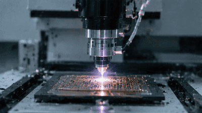
Advanced packaging has become one of the semiconductor industry’s most important growth engines, and it is now pulling a surprising set of process tools into the spotlight. Among the most in-demand are laser drilling and plasma dicing equipment. These machines sit close to the heart of heterogeneous integration, fan-out packaging, wafer thinning, TSV formation, glass substrate processing, and other advanced flows where precision, yield, and throughput matter enormously. As packaging moves from a back-end afterthought to a strategic platform, the equipment used to shape, open, and separate materials has become just as important as the dies themselves.

D2D Interface Bandwidth and Latency Comparison in Chiplet Architectures
Chiplet architecture has turned the package into a real performance battleground. Once multiple dies are placed side by side or stacked within the same advanced package, the quality of the die-to-die, or D2D, interface becomes one of the most important determinants of system behavior. Bandwidth is no longer a nice-to-have metric, and latency is no longer a small implementation detail. Together, they shape whether a chiplet system feels nearly monolithic or frustratingly fragmented.

Stock Selection Logic and Alpha Validation of ESG-Themed Semi ETFs
Semiconductor themed ETFs are no longer just about growth and cycles. A growing subset now layers environmental, social, and governance (ESG) criteria on top of traditional sector exposure. These ESG semi ETFs promise two things at once: access to one of the market’s most powerful secular themes, and alignment with sustainability and governance standards. The pitch is appealing, but it raises two hard questions. First, how exactly are these stocks being selected? Second, does the ESG overlay help, hurt, or leave alpha unchanged?